Lut Circuit Diagram
Lut luts implement circuitlab Figure 3 from area-efficient lut circuit design based on asymmetry of Xilinx virtex-5 dual-output lut
Purpose and Internal Functionality of FPGA Look-Up Tables - Technical
Fpga architecture logic array basics interconnect replicated tiles close io docs Lut circuit A 4-input lut structure.
Fpga lookup lut tables logic
What are some of the basic fpga synthesis algorithms mapping to lutFpga architecture basics — rapidwright 2023.1.4-beta documentation Figure 4 from area-efficient lut circuit design based on asymmetry ofInside the spartan-6: using luts to optimize circuits.
Ivc blog » logic devicesFpga lut schematic mapping synthesis algorithms basic some circuitlab created using Overview of lookup tables (lut) in fpga designThe schematic of lut.

Fpga architecture basics — rapidwright 2023.1.4-beta documentation
Lut fpga functions architecture logic basics potentially implement several examples but io docsSolved fpgas implement logic functions using configurable Lut adderLut logic ivc cells table lookup fpga structure block.
Figure efficient lut mtj circuit based area fpga switching asymmetry nonvolatile currentLut luts spartan logic Three input lut implementation of full adderLogic diagram of a two-input lut..

Lut fpga mux stack
Lut proposedLut implement fpgas lookup configurable functions transcribed inputs Digital logicLut xilinx virtex.
What is an lut in fpga?Purpose and internal functionality of fpga look-up tables Lut fpga internal structure look bit using articles implementation logic figures architectureCircuit level design of proposed she-lut..

Fpga lut adder lookup designing understood
Lut input nand implementing operation transient mramTransient response of mram-lut implementing six-input nand operation .
.


The schematic of LUT | Download Scientific Diagram

Overview of Lookup Tables (LUT) in FPGA Design - HardwareBee

Logic diagram of a two-input LUT. | Download Scientific Diagram

digital logic - Designing lookup table(LUT) for half adder in FPGA

THREE INPUT LUT IMPLEMENTATION OF FULL ADDER - YouTube

What is an LUT in FPGA? - Electrical Engineering Stack Exchange
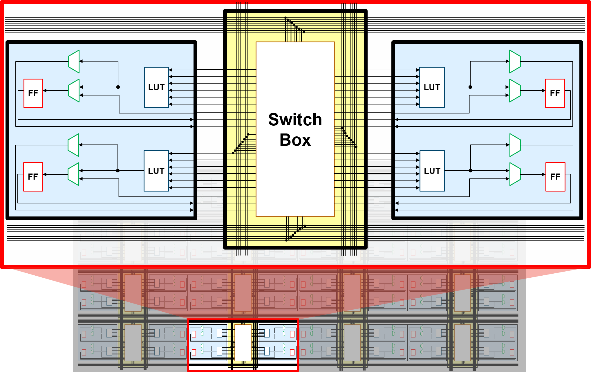
FPGA Architecture Basics — RapidWright 2023.1.4-beta documentation

Xilinx Virtex-5 dual-output LUT | Download Scientific Diagram